
10 MHz full bridge inverter
This board was designed to support both of my research projects by operating at either 6.78 or 10 MHz with a series resonant load. I started with four key criteria:
- minimize switching loop inductance
- minimize gate drive power, dead time, and switching times
- minimize logic-chain propagation delay
- design for low-voltage, high-current operation
Loop inductance is mostly a result of semiconductor packaging and pcb layout and I knew from the start I would be using GaN HEMTs, so I kept layout in mind as I selected the rest of the components. Resonant gate drives are gaining popularity in high frequency converter research but they don’t readily support the rapid on/off/on/off control necessary for the antenna amplifier, so I opted for a fast standard drive topology. This in mind, I selected the IGB110S10S1 from Infineon, a 100 V GaN device with only 3.4 nC gate charge and top-side cooling.
Another antenna project limitation is the need for galvanic isolation between the control and power circuits. This raises the minimum logic delay and results in three dead time options:
- isolated half-bridge driver
- driver with integrated dead time
- logic-side dead time circuit
- dual isolated drivers with a logic-side dead time circuit
- digital isolator with a non-isolated half bridge driver
- driver with integrated dead time
- separate dead time circuit (either side of the isolator)
The fastest isolated driver options come from Infineon, MPS, or Skyworks with 35-50 ns typical propagation delay. Those with integrated dead time did not go below 10 ns, and with only single driver outputs they offered no advantage over the dual-output single isolated drivers. Separating the isolation and gate drive allows much faster components for both, at the cost of dual output drivers. For this board I selected a MAX12930 dual channel isolator (5.6 ns delay, 50 kV/μs CMTI, and acceptably low skew) and LMG1210 half bridge driver (10 ns delay). The LMG1210 can use either internal or external deadtime with reasonable accuracy down to a few ns, switches at up to 50 MHz, and is compatible with either isolated or bootstrap high-side supplies. In revision 1, implemented both the internal deadtime and a resistor-capacitor-diode delay block for flexibility. I also utilized an isolated supply for the high-side driver to ensure symmetry. My starting component choices (which worked well after tweaking for component variability) were 10 ns external dead time, 5.1 ns internal dead time, and 2.2 ohm gate resistors (for a 4-5 ns rise/fall time).
The isolated supplies are Murata NXE2 series converters. Most importantly, they have very low isolation capacitance of only 2.1 pF. Despite a nominal 5 V output, they are unregulated and the no-load output can easily exceed my MAX12930 isolators’ maximum supply voltage. These Murata converters also tend to have high voltage ripple, some 10s of mV pk-pk. To solve both these issues I added an LC filter and 5.1 V zener for minimum loading.
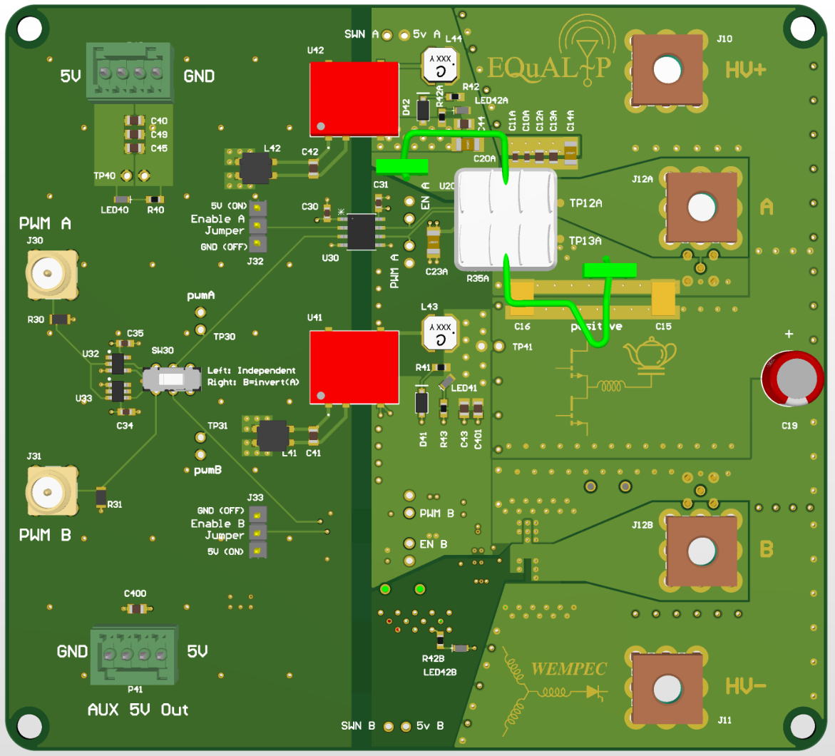
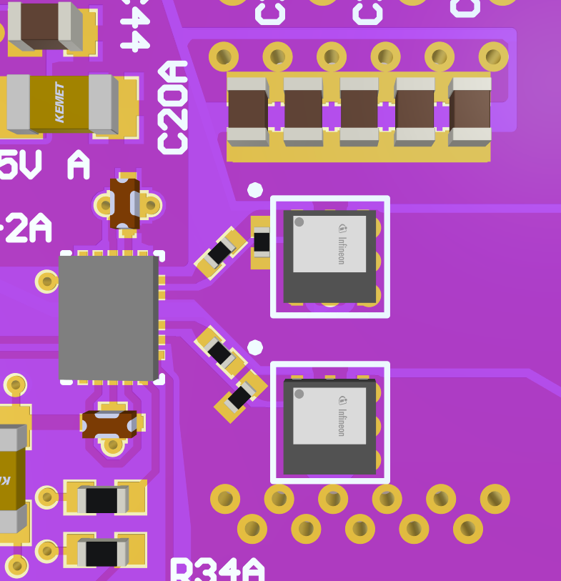
The board layout is a mixture of Ludois research group standards and my mission to shorten the switching loop. Existing projects dictated that I use screw terminals and those green terminal blocks, but I added my own touches with the SMA signal inputs and the second 5 V connector for auxiliary boards. I used first inner layer return and a sizeable decoupling bank for each half bridge, as shown in the next pair of photos.
The IGB110S10S1 has no kelvin source pin, but routing the switching node through the ground return path on the inner layer essentially turns the leftmost source pad into one (for high frequency currents, at least). There were a few minor problems with the first revision (purple boards), which I have revised for the second spin (green):
- The A and B bridges were not totally symmetrical, so it was difficult to tune a load for soft-switching both at the same time. This has been fixed with a totally symmetric mirror layout (bridge B is on the bottom side, mirrored about the center x axis)
- The local decoupling banks were too small, and I couldn’t find big enough 100V rated capacitors in 0805 footprint, especially considering limits on SRF.
- The discrete 10ns deadtime never got used, and the fuse was similarly unhelpful so both have been removed.
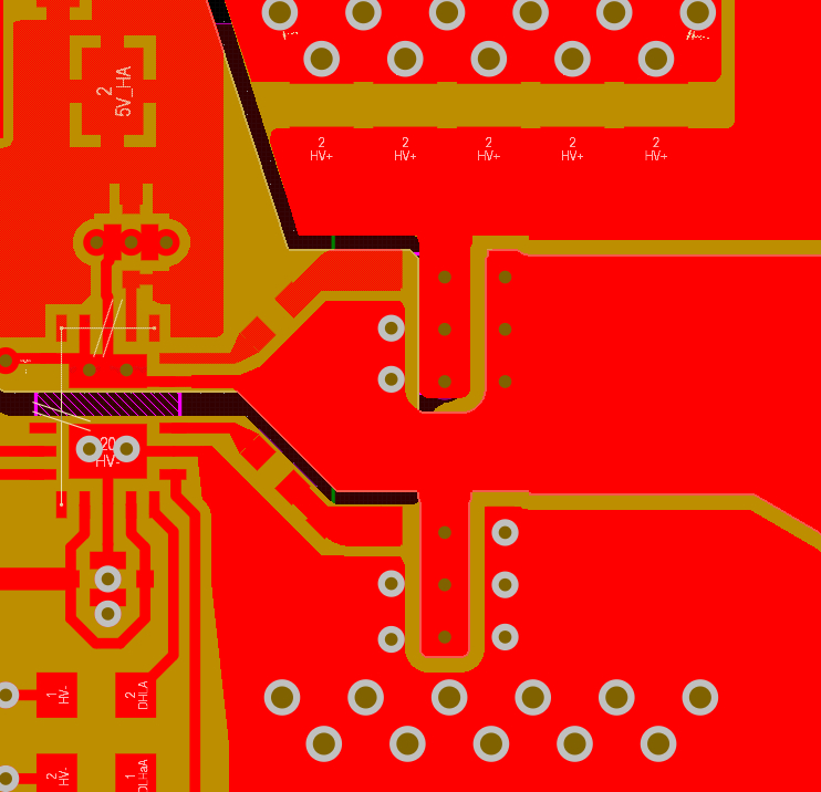
- Most importantly, there was too much capacitive coupling between the switch node and DC supply planes. This caused coupling between the two bridges and too much overshoot/undershoot when operating close to resonance. I have removed the ground planes under the switch node, and shortened the distance to the output connectors. The DC link now routes around the poles on the top and bottom layers.