
Phase-correct hysteresis controller
The goal is regulation of our non-LTI amplifier output power for root-raised-cosine pulse shaping. Prior work in the project was done with unregulated square pulse shapes, which allowed high symbol rates but did not suppress undesirable out-of-band radiation. The control scheme is similar in spirit to envelope elimination and restoration (EER) as proposed by Leonard Kahn, in that we separate the phase/frequency data modulation from pulse shape in order to drive a nonlinear amplifier. The system is optimized for phase-shift keying, and the current transmit symbol determines the phase of the carrier-frequency clock sent to the gate driver. Pulse width modulation is incompatible with RF class-D amplifiers (series resonant half- or full-bridge, not the audio kind) since departures from 50% duty prevent soft switching. This controller therefore uses hysteresis, or bang-bang, control. Kahn’s original and most contemporary EER systems rely on feedforward or predistortion optimized for a known load, e.g. 50 ohms. Ours is a closed-loop controller because it automatically accounts for deviations in load impedance arising from the electrically small antenna and single-element compensation network.
Controller Design
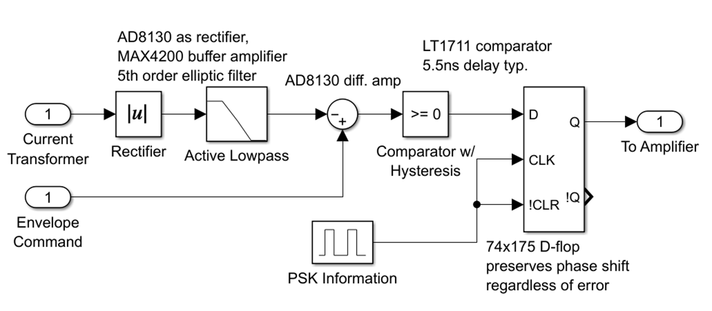
The first group is essentially a power detector. Antenna current is sensed by a current transformer (see web archives of G3YNH.info for details) connected to the controller. The sense voltage passes through an active half-wave rectifier, which uses an AD8130 for wide common-mode input range and fast slew rate. The AD8310 can only drive 30mA, so its output is buffered by the MAX4200 before the low pass filter. The filter is a 5th order elliptic with cutoff frequency around 2 MHz, and was chosen for maximum rejection of the 10 MHz carrier. This yeilds an approximation of the amplifier output power with precise bandwidth, which is not as easy to achieve with commercial power detector ICs.
The measured envelope is then subtracted from a command envelope to produce an error signal. The error is compared to zero with an LT1711 high-speed comparator. Previous controllers in this project used the LT1715 which has some hysteresis built-in, but it does not support arbitrary additional hysteresis about zero. The LT1711 has complementary outputs allowing for independent high and low trip levels set by positive feedback resistors.
Rather than let the error comparison directly switch the output to the gate drivers, it is buffered by a D type flip flop. This prevents gate pulses that start or end mid-cycle, which would cause hard switching and could potentially shift the phase of the output current and add communications error. While error is positive and the amplifier needs more power, a rising clock edge propagates this information from D to Q and then resets on the falling edge at the !CLR input, producing a gate pulse with the same duty cycle as the input clock. While error is negative, logic low at D prevents any pulses from reaching the gate driver. The simplicity of this design also allows it to control a class-E amplifier instead of class-D, if necessary.
Physical Implementation
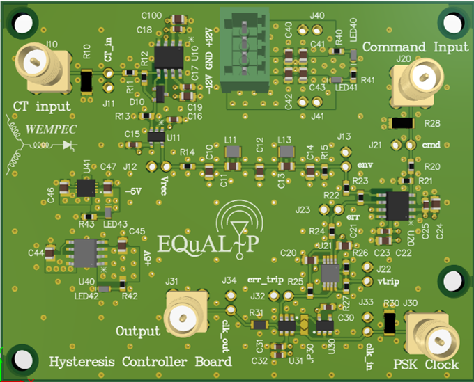
The layout is relatively straightforward, with all focus on simplifying the signal routing. It is a 4-layer board with signal on top and ground on the first inner layer. Power rails fill the bottom two layers, switching from \(\pm 12\) V to \(\pm 5\) V around the buffer and logic sections. Test points are in-line with the signal and can be optionally populated with 0.1” headers, making them maximally compatible with high-speed probes such as the Teledyne LeCroy DL-HCM. All coaxial terminals have optional 50 ohm termination sized for the expected power dissipation. The 12 V to 5 V conversion is managed by ADP7182 and ADP7118 linear regulators, which have PSRR bandwidths well above the 10 MHz carrier and harmonics.